

Nano electronics focuses on electronic devices, materials and systems designed and studied at extremely small dimensions. It sits at the intersection of electrical engineering, physics, materials science, nanotechnology and semiconductor technology.
For students interested in how modern chips, sensors, quantum devices and advanced computing technologies are developed, nano electronics can offer a highly specialised academic pathway. The field covers areas ranging from semiconductor devices and integrated circuits to quantum electronics, spintronics and neuromorphic systems.
Universities increasingly connect nanoelectronics education with laboratory research, nanofabrication and semiconductor applications. For example, current programmes at TU Delft and the University of Twente include semiconductor physics, integrated circuits, nanofabrication and nanoelectronics research, while EPFL offers a dedicated Nanoelectronics course within its Electrical and Electronics Engineering Master’s programme for 2026–27.
If you are considering studying nano electronics abroad in 2026/27, understanding the subject, curriculum, skills, destinations and career possibilities can help you choose a programme that matches your interests.
What Is Nano Electronics?
Nano electronics is the study and development of electronic components and systems whose important features operate at the nanoscale.
The nanoscale generally refers to dimensions below about 100 nanometres. At this scale, materials can exhibit electrical, magnetic and quantum behaviours that differ from what is observed in larger structures. The University of Twente, for example, describes nanoelectronics as the study of electronic and magnetic properties of systems with critical dimensions in the nanoregime, with research spanning areas such as quantum and neuromorphic electronics.
Nano electronics is closely related to microelectronics, but it places greater emphasis on nanoscale structures, emerging device concepts and the physical behaviour of materials and devices at very small dimensions.
The subject is particularly relevant to the semiconductor industry because modern electronic products depend on increasingly sophisticated semiconductor devices and integrated circuits.
The European Commission describes semiconductors as fundamental building blocks for electronic products and identifies chip design, manufacturing, packaging, research and skills development as important parts of Europe’s semiconductor ecosystem.
How Does Nano Electronics Work?
Nano electronics combines principles from electronics, semiconductor physics, materials science and nanotechnology to design and investigate extremely small devices.
Nano-Scale Electronic Devices
At the nanoscale, engineers and researchers study how electrons move through very small structures and how device characteristics can be controlled.
This can involve:
-
- Nano-scale transistors
-
- Quantum devices
-
- Nanoelectronic sensors
-
- Nanowires
-
- Single-electron devices
-
- Advanced memory concepts
-
- Nanoelectromechanical structures
- Nanoelectromechanical structures
The objective is not simply to make components smaller. Researchers also investigate new ways of controlling electrical, magnetic and quantum properties to create devices with useful functions.
Semiconductor and Integrated Circuit Technology
Semiconductors are central to modern electronics. Nano electronics therefore overlaps strongly with semiconductor device physics, integrated circuit technology and chip design.
Students may study topics such as:
-
- Semiconductor materials
-
- CMOS technology
-
- Transistor operation
-
- Integrated circuit design
-
- Device fabrication
-
- Device characterisation
-
- Circuit testing
-
- VLSI systems
-
- Semiconductor manufacturing
- Semiconductor manufacturing
TU Delft’s MSc Microelectronics, for example, covers areas including semiconductor device physics, digital IC design, analog CMOS design and integrated circuits and MEMS technology.
Emerging Nanoelectronics Technologies
Nanoelectronics also extends beyond conventional silicon electronics.
Depending on the programme, students may encounter:
-
- Quantum electronics
-
- Spintronics
-
- Neuromorphic electronics
-
- Carbon nanotube electronics
-
- Single-electron devices
-
- Quantum-dot-based systems
-
- Advanced semiconductor devices
- Advanced semiconductor devices
EPFL’s 2026–27 Nanoelectronics course includes topics such as tunnel FETs, negative-capacitance switches, quantum-dot cellular automata, carbon nanotubes and spintronics.
What Do You Study in a Nano Electronics Course?
There is no single universal nano electronics curriculum. Course content varies according to whether the programme is positioned within electrical engineering, physics, nanotechnology, materials science or semiconductor engineering.
Common subjects can include:
| Study Area | What Students May Learn |
|---|---|
| Semiconductor Physics | Electronic properties and behaviour of semiconductor materials |
| Nanoelectronics | Nanoscale electronic and magnetic systems |
| Integrated Circuits | Design and operation of electronic circuits |
| Device Physics | Principles behind semiconductor devices |
| Nanomaterials | Materials used in nanoscale devices |
| Nanofabrication | Techniques for manufacturing nanoscale structures |
| Quantum Electronics | Electronic systems influenced by quantum effects |
| Chip Design | Designing and evaluating integrated circuits |
| Characterisation | Measuring and analysing device properties |
| Research Methods | Designing experiments and interpreting results |
For example, the University of Twente’s Nanoelectronics specialisation includes materials science, nanoelectronics, semiconductor device physics and integrated circuit technology, alongside electives and research-based work. Students also complete an internship and Master’s thesis.
Semiconductor Physics and Device Engineering
Semiconductor physics helps students understand how electronic devices function at the material and device level.
Topics may include:
-
- Charge carriers
-
- Semiconductor junctions
-
- Transistors
-
- Energy bands
-
- Electronic transport
-
- Device modelling
-
- Advanced semiconductor structures
- Advanced semiconductor structures
A strong understanding of physics can be particularly useful for students interested in research and device development.
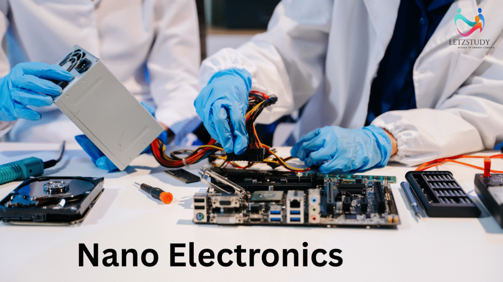
Integrated Circuits and Chip Design
Students interested in the design side of nano electronics may explore integrated circuit architecture, analog and digital circuits, CMOS technologies and testing.
This pathway can suit students who want to combine device knowledge with electronics design and computational tools.
Nanomaterials and Fabrication
Nanoelectronics requires specialised methods for creating and studying very small structures.
Depending on the university, students may receive exposure to:
-
- Cleanroom processes
-
- Lithography
-
- Thin-film deposition
-
- Etching
-
- Material characterisation
-
- Device fabrication
-
- Experimental measurement
- Experimental measurement
The University of Twente’s NanoElectronics group, for example, provides students with opportunities to work on nanofabrication, characterisation and modelling, including cleanroom work involving electron-beam lithography and thin-film equipment.
Quantum and Emerging Electronics
Students interested in next-generation computing and devices can explore quantum electronics, neuromorphic systems and other emerging technologies.
These areas are often research-oriented, so students should expect a strong emphasis on mathematics, physics, experimentation and independent investigation.
What Skills Do You Need for Nano Electronics?
A successful nano electronics student typically needs a combination of technical, analytical and laboratory skills.
Technical Skills
Useful foundations include:
-
- Electrical and electronic engineering
-
- Semiconductor physics
-
- Mathematics
-
- Materials science
-
- Circuit analysis
-
- Programming
-
- Device modelling
-
- Electronics laboratory techniques
- Electronics laboratory techniques
Programming can be useful for simulation, data analysis, modelling and automation, although the specific software requirements depend on the programme.
Research and Laboratory Skills
Nanoelectronics is strongly connected to experimental research. Students may need to develop skills in:
-
- Experimental design
-
- Data interpretation
-
- Device measurement
-
- Microscopy and characterisation
-
- Nanofabrication
-
- Technical documentation
-
- Scientific communication
Problem-Solving Skills
At the nanoscale, small changes in materials, structures and fabrication conditions can influence device performance. Strong analytical thinking and attention to detail are therefore valuable.
Why Study Nano Electronics Abroad in 2026/27?
Studying nano electronics abroad can provide access to specialised laboratories, research groups, advanced semiconductor facilities and international academic environments.
One reason the field is receiving continued attention is the strategic importance of semiconductor technology. The European Commission’s 2026 proposal for a Chips Act 2.0 focuses on strengthening semiconductor research, design, manufacturing capabilities, skills and supply-chain resilience in Europe.
For students, this wider ecosystem can make it useful to consider universities not only by course title but also by their:
-
- Semiconductor research facilities
-
- Cleanroom access
-
- Industry collaborations
-
- Research projects
-
- Internship opportunities
-
- Master’s thesis options
-
- Links with semiconductor companies
-
- Specialisations in emerging technologies
Where Can You Study Nano Electronics Abroad?
Nanoelectronics may not always appear as the exact name of a full degree. It can instead be offered as a specialisation, track, course or research area within programmes such as Electrical Engineering, Microelectronics, Nanotechnology, Applied Physics or Semiconductor Engineering.
Netherlands
The Netherlands is an important option for students interested in microelectronics and nanotechnology.
TU Delft offers an MSc Microelectronics programme that runs for 24 months and is taught in English. The programme combines theoretical study, laboratory work, specialisation courses and a substantial graduation project. Its scope includes the design, fabrication and testing of devices, circuits and systems using integrated microfabrication technologies.
University of Twente offers nanoelectronics within its Electrical Engineering Master’s pathway and also has a broader Master’s in Nanotechnology. Its Nanoelectronics specialisation combines electrical engineering with physics, materials science and nanotechnology, with opportunities for internships and thesis research.
Switzerland
Switzerland can also be considered by students looking for advanced electronics and nanotechnology research.
EPFL includes Nanoelectronics in its Electrical and Electronics Engineering Master’s curriculum for 2026–27. The course covers emerging device concepts and technologies including tunnel FETs, carbon nanotubes and spintronics.
Other Semiconductor and Nanotechnology Study Destinations
Depending on the exact specialisation, students can also investigate universities and research-focused programmes in countries such as:
-
- Germany
-
- France
-
- Belgium
-
- United Kingdom
-
- United States
-
- Japan
-
- South Korea
-
- Taiwan
-
- Singapore
- Singapore
The right destination depends on whether your priority is chip design, semiconductor manufacturing, nanomaterials, quantum technology, device physics or research.
What Are the Applications of Nano Electronics?
Nanoelectronics contributes to technologies across several industries.
Consumer Electronics
Smaller and more capable electronic components support smartphones, computers, wearable devices and other connected products.
Artificial Intelligence and Computing
Advanced semiconductor technologies are important for the computing infrastructure used by AI and other data-intensive applications. The European Commission’s 2026 semiconductor strategy specifically connects advanced chips with AI, cloud infrastructure and other emerging digital technologies.
Healthcare
Nano-scale electronic devices can contribute to sensors, diagnostic technologies, biomedical devices and lab-on-a-chip systems.
Automotive Technology
Modern vehicles depend on large numbers of semiconductor components for control, sensing, communication and computing.
Quantum Technology
Nanoelectronics can support research into quantum devices and quantum information technologies.
Energy and Sensors
Nano-scale materials and devices can also contribute to sensing, energy technologies and other applications where small size and specialised material properties are important.
Nano Electronics Career Opportunities
A nano electronics qualification can lead to several technical and research-oriented career directions.
Potential roles include:
-
- Semiconductor device engineer
-
- Nanoelectronics engineer
-
- Microelectronics engineer
-
- IC design engineer
-
- Semiconductor process engineer
-
- Device characterisation engineer
-
- Hardware engineer
-
- Research engineer
-
- Nanotechnology engineer
-
- Semiconductor test engineer
-
- Materials or process specialist
-
- R&D engineer
- R&D engineer
Career outcomes depend on the student’s qualification level, technical specialisation, practical experience and the requirements of individual employers.
Students who continue to doctoral study may pursue research careers in universities, semiconductor laboratories or industrial R&D organisations.
Nano Electronics vs Microelectronics: What Is the Difference?
The two fields overlap considerably, but their emphasis can differ.
| Nano Electronics | Microelectronics |
|---|---|
| Focuses strongly on nanoscale electronic systems | Covers electronic systems using microfabrication technologies |
| Often explores emerging device concepts | Strongly connected with established semiconductor technologies |
| May include quantum, spin and neuromorphic electronics | Commonly includes IC design, semiconductor devices and systems |
| Strong connection with nanotechnology and materials science | Strong connection with electrical and computer engineering |
| Often research-intensive | Can range from design and manufacturing to systems engineering |
The distinction is not absolute. Many university programmes combine microelectronics and nanoelectronics, and students may move between the two areas depending on their specialisation.
How to Choose the Right Nano Electronics Programme
Before applying, compare programmes beyond their titles.
Consider these factors:
-
- Academic background: Check whether the programme expects electrical engineering, electronics, physics, materials science or another related degree.
-
- Curriculum: Look for subjects that match your interests, such as semiconductor physics, IC design, nanofabrication or quantum electronics.
-
- Laboratory facilities: Check whether students have access to cleanrooms, fabrication equipment and device-characterisation facilities.
-
- Research opportunities: Review faculty research groups and current thesis topics.
-
- Industry exposure: Look for internships, industrial projects and collaborations with semiconductor companies.
-
- Programme structure: Compare coursework, laboratory work, internships and thesis requirements.
-
- Language: Confirm the language of instruction and any language requirements.
-
- Career direction: Choose a programme that supports your intended path, whether it is chip design, manufacturing, R&D or doctoral research.
-
- Admission requirements: Check the university’s current requirements rather than relying on general eligibility rules.
-
- Total study-abroad budget: Compare tuition, accommodation, insurance, travel and living expenses using current university and government information.
- Total study-abroad budget: Compare tuition, accommodation, insurance, travel and living expenses using current university and government information.
For example, TU Delft’s Microelectronics programme includes a substantial graduation project, while the University of Twente’s Nanoelectronics pathway includes an internship and Master’s thesis. These differences can significantly affect the type of practical experience you gain.
Common Challenges to Consider
Nano electronics can be academically demanding. Students should be prepared for:
-
- Strong mathematics and physics requirements
-
- Complex semiconductor concepts
-
- Laboratory-based learning
-
- Research-intensive projects
-
- Detailed technical analysis
-
- Rapidly evolving semiconductor technologies
-
- Competition for specialised roles
- Competition for specialised roles
It is also important not to choose a programme simply because “nanoelectronics” sounds technologically advanced. Review the actual modules, facilities, research groups and career relevance before applying.
FAQs
What is nano electronics?
Nano electronics is a branch of electronics concerned with electronic and magnetic systems at nanoscale dimensions. It combines areas such as electrical engineering, physics, materials science and nanotechnology.
Is nano electronics a good field to study in 2026/27?
It can be a suitable field for students interested in semiconductors, advanced electronic devices, chip technologies, nanotechnology and emerging areas such as quantum and neuromorphic electronics. The suitability depends on your academic background and career goals.
What degree is needed to study nano electronics?
Requirements vary by university. Related backgrounds can include electrical or electronics engineering, physics, applied physics, materials science, nanotechnology and other closely related disciplines.
Where can I study nano electronics abroad?
Nanoelectronics can be studied through specialised courses, tracks or programmes in countries including the Netherlands and Switzerland, as well as through related semiconductor, microelectronics and nanotechnology programmes in other major technology destinations.
What skills are useful for a career in nano electronics?
Useful skills include semiconductor physics, electronics, mathematics, programming, circuit design, materials science, laboratory techniques, device characterisation and research skills.
What is the difference between nanoelectronics and nanotechnology?
Nanotechnology is a broader multidisciplinary field concerned with structures and materials at the nanoscale. Nanoelectronics specifically focuses on electronic and related device applications at these very small dimensions.
Key Takeaways
Nano electronics brings together electronics, semiconductor technology, physics, materials science and nanotechnology to investigate and develop electronic systems at extremely small scales. For students planning to study abroad in 2026/27, the field can offer pathways into semiconductor devices, chip design, nanofabrication, quantum electronics and advanced R&D.
When choosing a programme, look beyond the course title. Compare the curriculum, laboratory facilities, research opportunities, industry exposure, admission requirements and career relevance. A carefully selected programme can help you build the specialised knowledge needed for an evolving semiconductor and electronics landscape.
Start Your Study Abroad Journey
If you are planning to study abroad and need help understanding your options, you can connect with a LetzStudy counsellor for personalised guidance. We can help you explore suitable countries, universities, courses, eligibility requirements, application steps and other aspects of your study-abroad journey based on your academic profile and goals.
